
A combinational circuit is circuit whose output is determined solely by the current state of its inputs. A sequential circuit is a circuit whose output is determined by the current state of its inputs and its previous output. In general, a sequential circuit is composed of a combinational circuit and a memory unit whose value is the output of the circuit.
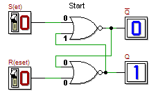
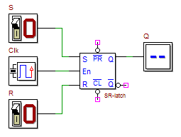
A latch is an asynchronous sequential circuit; a circuit that responds immediately to changes in the values of its input signals. An SR Latch (see the illustration below) has two inputs (S and R) and two outputs (Q and Q'). For the most part, we will refer to Q as the output with the understanding that Q' has the opposite value. The S (set) input sets the output to 1 and the R (reset) input resets the output to 0. If R and S are both low (as they normally are), the circuit maintains its previous output value. However, if R and S are both set high, both Q and Q' go to 0. Furthermore, if S and R are then simultaneously returned to 0 then the circuit becomes unstable. Because of these undesirable properties, S = 1 and R = 1 is called the forbidden state.
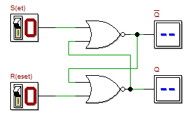
When this circuit is first turned on, the outputs are indeterminate since we don't know whether Q will be 0 or 1. Since the outputs are indeterminate and these outputs also serve as inputs to the NOR gates, the circuit remains in an indeterminate state until it is set or reset.
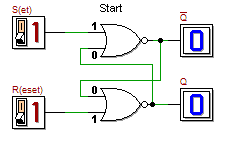
The SR latch is set when S = 1 and R = 0. When a latch is set, the output Q is set to 1. Suppose Q is already 1 as illustrated below. Setting S to 1 doesn't change the output of the upper NOR gate so the output remains Q = 1.
Now, let's suppose that Q is 0 when S is set to 1 (see illustration below). The following sequence occurs:
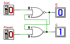
The SR latch is reset when S = 0 and R = 1. When a latch is reset, the output Q is set to 0. Suppose Q is already 0 as illustrated below. Setting R to 1 doesn't change the output of the lower NOR gate so the output remains Q = 0.
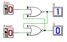
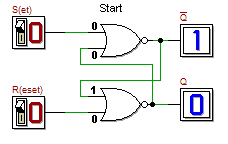
Now, let's suppose that Q is 1 when R is set to 1 (see illustration below). The following sequence occurs:

Suppose the latch's output is 1 and S and R both go to 1 as illustrated below.
A similar sequence of events would occur if Q was 0 when S and R were both set to 1.
The real problem arises when the inputs R and S are both set back to 0 simultaneously (as shown below). The following sequence of events takes place:
In summary, an SR latch has the following behavior:
| S | R | Output |
| 0 | 0 | Stable |
| 1 | 0 | 1 |
| 0 | 1 | 0 |
| 1 | 1 | Forbidden |
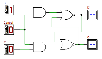
An SR latch with control is shown below. In this circuit, the S and R inputs are enabled by a control signal. When the control signal is low, the inputs to the latch are inhibited and the latch "sees" both of its inputs as being low; the stable state. When the control signal is high, the inputs are enabled and the latch responds normally.
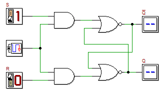
For a clocked SR latch, the control signal is a clock; a signal that alternates between high and low on a regular periodic basis. For the clocked SR latch shown below, the inputs are enabled only when the clock signal is high. Such a latch is said to be level triggered since whether it is enabled or not is determined by the level of the clock signal.
The basic clocked SR latch is a basic building block for more complicated
circuits and is represented as a single component in the illustration below.
There are two inputs that we have not discussed. The
![]() signal
is used to pre-set the output of the latch to 1 asynchronously. The fact
that the input is shown as a complement indicates that it is active low.
That is, when this signal is high, it has no affect on the latch. Whenever
this signal is low, the output of the latch will be 1. The
signal
is used to pre-set the output of the latch to 1 asynchronously. The fact
that the input is shown as a complement indicates that it is active low.
That is, when this signal is high, it has no affect on the latch. Whenever
this signal is low, the output of the latch will be 1. The
![]() signal clears the
latch. When this signal is high, it has no effect. Whenever this signal is
low, the output of the latch will be 0. Obviously, it would be a mistake to
set both of these signals low at the same time. One use of these input
signals is to set the latch into a predetermined state during the boot-up
sequence.
signal clears the
latch. When this signal is high, it has no effect. Whenever this signal is
low, the output of the latch will be 0. Obviously, it would be a mistake to
set both of these signals low at the same time. One use of these input
signals is to set the latch into a predetermined state during the boot-up
sequence.
A clocked SR latch is a synchronous circuit (assuming that the inputs do not change while the clock is high). Multiple synchronous circuits in a complex design all respond to their inputs at the same time (i.e., when the clock signal goes high). In practice, it is difficult to ensure that the inputs will not change while the clock is high leading to the necessity of a more sophisticated circuit.
In general, a flip-flop is an edge-triggered latch. An edge-triggered circuit is triggered by a transition in the clock signal from low to high (positive or leading edge) or by the transition from high to low (negative or trailing edge). A master-slave flip-flop is constructed from two clocked SR latches as shown here:
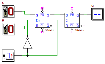
Notice that the first latch is level-triggered by a low clock signal and the second latch is level-triggered by a high clock signal. When the clock is low, the S and R inputs are free to propagate through the first latch but the second latch is disabled freezing its outputs. When the clock goes high, the first latch is disabled freezing its output values which can now propagate through the enabled second latch. Notice, that while the clock is high, the S and R inputs can change (in preparation for the next cycle) but because the first latch is disabled, those changes will not affect anything until the clock goes low again.
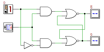
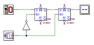
A clocked D latch is constructed by modifying the inputs to an SR latch. As illustrated below, there is only one input (D) which replaces the S input. The complement of D replaces the R input. In effect, we are eliminating the S = 0 and R = 0 state and the forbidden S = 1 and R = 1 state. The output of this latch is the value of D. This latch is level-triggered and will respond to changes in D as long as the clock signal is high.
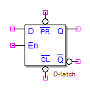
A D latch with control can be represented as a single component as shown
below. As discussed earlier the ![]() and
and ![]() inputs allow the latch to
be preset to 1 or cleared to 0. Both inputs are active low. The En input is
the enable input which can be wired to a clock signal if desired.
inputs allow the latch to
be preset to 1 or cleared to 0. Both inputs are active low. The En input is
the enable input which can be wired to a clock signal if desired.
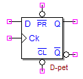
A D Flip-Flop (see illustration below) is an edge-triggered circuit that can be constructed from two clocked D latches much as the master-slave flip-flop was constructed.
A positive edge triggered D flip-flop can be represented as a single component as shown below:
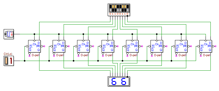
A register is used to store a multi-bit binary number. It utilizes a flip-flop for each bit with all of the flip-flops having a common clock signal and a common clear signal. In the illustration below, the inputs to the register come from the dipswitch at the top. The input at the lower left is the clear signal which is active low. When the computer boots up, this signal would go low momentarily initializing the register to all zeroes. The output of the register is displayed as a two-digit hexadecimal number.
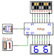
As you might guess, an 8-bit register can also be represented as a modular building block:
Typically, a central processing unit (CPU) contains several registers any one of which can be used as an input to the arithmetic logic unit (ALU). Suppose a CPU contains 4 general purpose registers (R0, R1, R2, and R3) and the ALU has two input registers (A and B). The CPU must contain a circuit that routes one of these 4 general purpose registers to the the A register of the ALU and another circuit to route one of these 4 registers to the B register of the ALU. Recall that a circuit that routes one of its inputs to its output is called a multiplexer.
The drawing below illustrates a CPU with four 4-bit registers. (The dip switches that provide the inputs to these registers are labeled rather than the registers themselves.) Control lines A1 and A0 determine which register is sent to the A register of the ALU. Control lines B1 and B0 determine which register is sent to the B register of the ALU. (The output LEDs for these registers are labeled rather than the registers.)
The low-order bits from each of the four registers are the input to the upper multiplexer on the A (left) side of the circuit. This multiplexer selects one of these bits as its output based on the select signals A1 and A0. The next multiplexer down determines which bit in the 2's column is selected. The third multiplexer selects the 4's bit and the bottom multiplexer chooses the 8's bit (the most significant bit). Since the control lines A1 and A0 are wired the same way in every multiplexer, all four bits selected will come from the same register. The selected bits serve as the inputs to the A register. This same pattern is repeated on the right side of the circuit which selects which register has its contents copied to the B register.
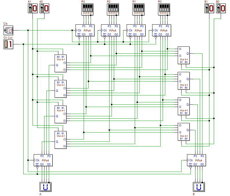
If you have the DEEDS digital circuit simulator you can download RegMultiplexer4.pbs and play with this circuit.
The result generated by the ALU is stored in another register whose bit pattern is usually routed to one of the four general purpose registers in the CPU. Recall that a circuit that routes its input to one of several possible outputs is called a demultiplexer. The construction of this circuit is left as an exercise.
Conceptually, memory consists of a large collection of low-speed registers. (Since a register is understood to be a high-speed storage unit, I guess the term "low-speed register" is an oxymoron.)
Consider the very, very simple memory illustrated below. This memory consists of four 4-bit words. The inputs D0 through D3 come from the data bus of the computer. Notice that each input bit is wired to the corresponding bit position of all 4 words of memory. The output of this memory (Output0 through Output3) is also connected to the data bus. The data bus can be used to write data to memory or read data from memory but not both at the same time (think XOR).
The signals A0 and A1 come from the address bus and serve as an input to a decoder which selects the corresponding word of memory. In particular, the output of the decoder enables several AND gates. The left-most AND gate enables a leading edge trigger to reach the clock input of each flip-flop in the selected word. If that happens a write operation occurs. The other four AND gates enable the output of the selected word to be transferred to the OR gates at the bottom of the diagram. If that happens, the data in the word can be read. Notice that if a word is not selected, all of its D latches are disabled; they can not receive new data because the clock signal is disabled and they are disconnected from the data bus since their outputs are disabled.
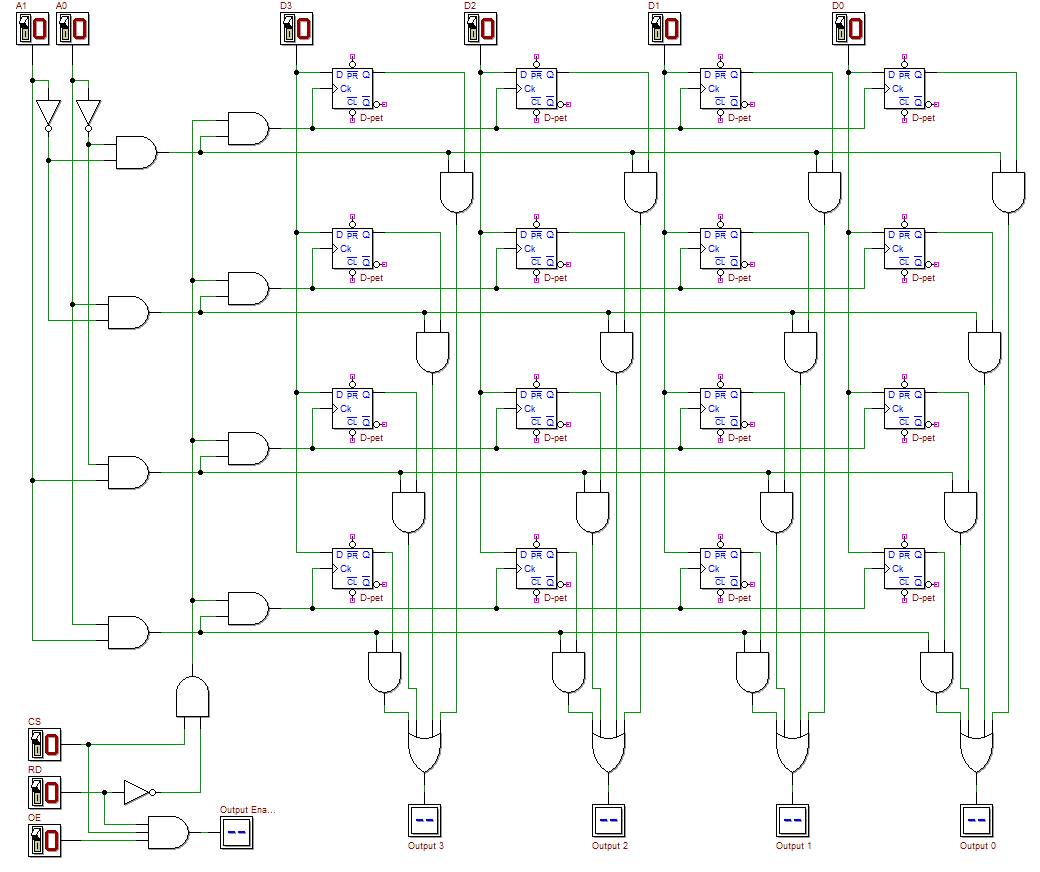
If you have access to the DEEDS digital circuit simulator software, you can download Memory.pbs and play with this circuit.
The three signals at the bottom left control the operation of this memory unit. The CS (Chip Select) signal is active high. That is, if CS goes high, then the memory unit is enabled. Otherwise, the entire unit is disabled. In a computer with multiple memory units, part of the address of a memory location drives a decoder which selects the particular memory unit in which the desired word is located. The desired word is located within the memory unit based on the inputs to the address decoder as described above.
The CS signal is wired to the inputs of two AND gates. The upper AND gate controls whether data will be written to the memory unit. A write operation can occur only if the CS signal is high. The lower AND gate determines whether a read operation can occur. A read operation can occur only if the CS signal is high.
The RD (Read) signal determines whether the memory is in read mode (RD = 1) or write mode (RD = 0). The RD signal is wired to the input of an AND gate and a NOT gate. The AND gate determines whether a read operation will occur. A read operation can occur only if the RD signal is high. The output of the NOT gate is wired to the input of the AND gate that determines whether a write operation will be performed. A write operation can be performed only if the RD signal is low (and, as a result, the signal from the NOT gate is high).
The OE (output enable) signal is active high and is wired to the AND gate the determines whether a read operation will occur. A read operation can occur only if the OE signal is high.
In summary, these three control signals control what operation will be performed:
| Chip Select | Read | Output Enable | Operation |
| 0 | X | X | Disabled |
| 1 | 0 | X | Write |
| 1 | 1 | 0 | Nothing |
| 1 | 1 | 1 | Read |
Let's look at what happens during a write operation:
While all of this is going on, the output of the selected word is sent to the OR gates at the bottom of the diagram but since the RD signal is low, that data is not transferred to the data bus.
Now consider what happens during a read operation:
While all of this is going on, the AND gate controlled by CS and RD remains low so no leading edge is transmitted to the selected word of memory and, consequently, no write operation is performed.
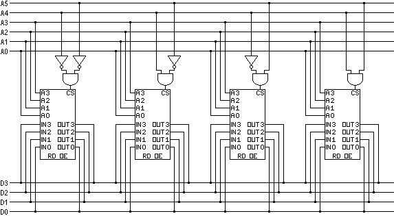
Memory chips come in a number of different designs. As a very simple example, consider a computer with 4-bit words and memory chips that contain 64 bits. The list below indicates some possible organizations for this chip. Each chip could have
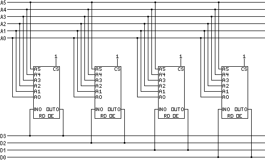
To continue the example suppose the address space of the computer consisted of 64 4-bit words. That is, the computer has six address lines. If the 4-bit memory chips are used, this computer could have memory sizes of 16, 32, 48, or 64 words. A full 64 word memory is illustrated below. Smaller memories can be made by eliminating memory chips (starting at the right side).
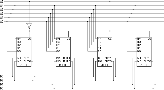
If 2-bit memory chips were used, it would take two chips to form a complete 4-bit word. Consequently, the memory chips would have to be used in pairs and the possible memory sizes would be 32 or 64 words. A full 64 word memory is illustrated below. Notice that the first bank of two chips is selected when A5 is low and the second bank of two chips is selected when A5 is high. Removing the two chips on the right would yield a 32-word memory.
If 1-bit memory chips were used, it would take four chips to form a complete 4-bit word and the only memory size possible would be 64 words. Because the full 6-bit address is decoded by each memory chip, the CS input can be wired so it is permanently high. Each memory chip is always selected.
While actual memory chip have much larger capacities, these basic principles still apply. However, the number of address lines and data lines would be much larger.